Finding decent switches is hard: most of the modern offerings seem to suffer from the current disease of “If it needs a web interface, put Linux on it”. That’s fine for something like a router, but having your switch take minutes to boot isn’t. I also detest switches where it’s easy to leave the switch in a state where the current running configuration is different from the configuration that will be used at the next boot – plunging your network into disarray at the next power cut.
D-Link used to sell an excellent set of Web/SNMP manageable switches which they called DGS1216/24/48T. They boot in seconds, and you can usually pick them up on eBay for about £30 – there are multiple versions of the hardware, this article deals with the D1/D2 revision of the 16 port version.
A few of the ones I bought recently had a peculiar pathology: after updating the firmware they would run fine (complete with working UI), and then about 100 seconds after power on, they would freeze and stop forwarding traffic. Given they’d worked fine before the firmware update I assumed it wasn’t a hardware problem. After I had 3 of them in this state, I decided to take a quick look and see if the problem was anything obvious, or if I could just downgrade the firmware with an EEPROM programmer. The first step was to get the lid off. Here’s a side lit (so you can read the chips) picture of the right hand side of the board:
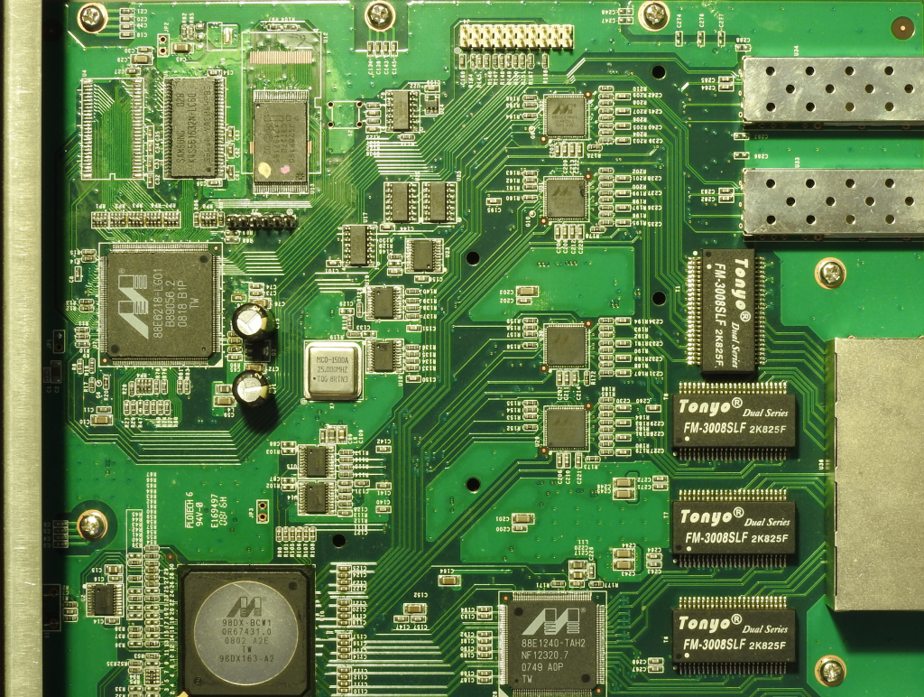
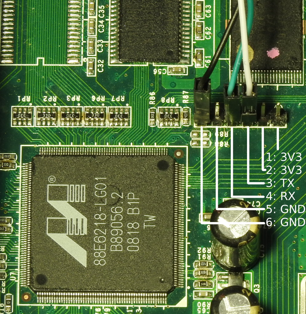
The first thing to notice is that are two headers (which I’ve populated). J3, black and at the top-left, turns out to be a serial port:
A little bit of Googling suggests that the Marvel 88E6218 is an ARM9E based CPU, and sure enough, at 38400 baud, the serial port says:
Hit any key for boot setup
ARMboot code: +_armboot_start 00380000 -> 00392180
At the moment the switch becomes sad and stops forwarding traffic the serial port says:
Prestera commander shell server ready
***************************************
->Port 0 is Link up

MAC illegal
Ordinarily the next step would be to start tearing apart the firmware image of the switch, but there’s that promising other 20 pin header. There’s a canonical 20 pin ARM JTAG header, and sure enough that’s what it is. I connected a SEGGER J-Link and after a bit of trial and error wrote a board configuration file mapping out the RAM and the ROM. I dumped the ROM with:
[lab@lab dgs1216t]$ openocd -f openocd-dgs1216t.cfg -c init -c halt -c 'dump_image rom.bin 0xffe00000 0x00200000' -c shutdown
Open On-Chip Debugger 0.9.0 (2016-02-05-11:44)
Licensed under GNU GPL v2
...
target halted in ARM state due to debug-request, current mode: Supervisor
cpsr: 0x20000013 pc: 0x000c4958
dumped 2097152 bytes in 66.150436s (30.960 KiB/s)
shutdown command invoked
[lab@lab dgs1216t]$
and then searched for the string ‘MAC illegal’, but found nothing; it’s likely the bootloader is unpacking an image stored in the ROM. So instead I dumped a RAM image after the switch had booted. The location of the RAM in the memory map can be intuited by running strings(1) on the ROM image:
sdramImgAddr=0x00100000
board_cmd_sdramsize=0x800000
so
[lab@lab dgs1216t]$ openocd -f openocd-dgs1216t.cfg -c init -c halt -c 'dump_image ram.bin 0x0 0x00800000' -c shutdown
Open On-Chip Debugger 0.9.0 (2016-02-05-11:44)
Licensed under GNU GPL v2
...
Info : JTAG tap: dgs1216t.cpu tap/device found: 0x159463d3 (mfg: 0x1e9, part: 0x5946, ver: 0x1)
Info : Embedded ICE version 5
Info : 88e6218: hardware has 2 breakpoint/watchpoint units
dumped 8388608 bytes in 190.316849s (43.044 KiB/s)
shutdown command invoked
And the RAM image does contain the magic string “MAC illegal”:
00121cb0  6d 65 72 28 29 2d 2d 43  61 6e 27 74 20 73 74 61  |mer()--Can't sta|
00121cc0  72 74 20 74 69 6d 65 72  0a 00 00 00 69 4c 6f 76  |rt timer....iLov|
00121cd0  45 44 6c 69 6e 4b 53 77  69 54 63 48 00 00 00 00  |EDlinKSwiTcH....|
00121ce0  4d 41 43 20 69 6c 6c 65  67 61 6c 0a 00 00 00 00  |MAC illegal.....|
00121cf0  74 72 75 6e 6b 74 6d 72  2e 63 2d 2d 53 74 61 72  |trunktmr.c--Star|
00121d00  74 5f 43 68 65 63 6b 5f  48 6d 61 63 5f 54 69 6d  |t_Check_Hmac_Tim|
To find the bit of code that’s causing the trouble we search for the address, 0x121ce0, of the string. It occurs exactly once at 0x9ab4, and the dissassembly looks like:
0x9a90: cmp     r3, #0
0x9a94: beq     0x9ab8
0x9a98: ldr     r0, [pc, #20]   ; 0x9ab4
0x9a9c: bl      0xc20b4
0x9aa0: bl      0x99b0
0x9aa4: mov     r0, #2
0x9aa8: bl      0x93f4
0x9aac: b       0x9ab8
0x9ab0: .dword  0x121ccc
0x9ab4: .dword  0x121ce0
0x9ab8:
Now one of the nice things about ARM JTAG is that there’s also a full on-chip debugger. So gdb can set a breakpoint at 0x9a90 and see what happens if the CPU is forced to take the other branch in the test.
[lab@lab dgs1216t]$ arm-none-eabi-gdb
GNU gdb (GDB) 7.6.2
[...]
(gdb) target remote localhost:3333
Remote debugging using localhost:3333
0x00111f14 in ?? ()
(gdb) hbreak *(0x9a90)
Hardware assisted breakpoint 1 at 0x9a90
(gdb) set $pc=0xffff0000
(gdb) cont
Continuing.
Breakpoint 1, 0x00009a90 in ?? ()
(gdb) p $r3
$1 = 15
(gdb) set $r3=0
(gdb) cont
Continuing.
I’ve not added a reset method to the OpenOCD configuration file so a “poor man’s reset” of jumping to the start of the boot code in ROM is used, and since the boot-loader overwrites the code in RAM, hardware breakpoints have to be used.
After setting the register and taking the other branch in the test, the switch behaves normally. It would be possible to patch out this test in the ROM, but that’s going to require reverse engineering the unpacking code and even then the switch won’t work if the firmware is upgraded. A better solution requires looking more carefully at the function containing the test. I’m indebted to a friend who is much quicker at reading ARM assembly than I am, for helping me render it into the following:
void
func_99d8 (void)
{
  uint8_t L32[32];
  int L36;
  uint8_t L44[8];
  uint8_t L60[16];
  uint8_t L76[16];

  memcpy (L32, "iLovEDlinKSwiTcH", 17);

  L36 = 0;

  if (func_5eeec ())
    return;

  func_1f234 (L44);
  memset (L60, 0, 16);
  func_5ed88 (L44, L32, L60);
  func_c192c (L76, 16);

0x9a74: sub     r3, fp, #60     ; L60
0x9a78: sub     r2, fp, #76     ; L76
0x9a7c: mov     r0, r3
0x9a80: mov     r1, r2
0x9a84: mov     r2, #16
0x9a88: bl      0x1159bc        ; memcmp
0x9a8c: mov     r3, r0
0x9a90: cmp     r3, #0
0x9a94: beq     0x9ab8

  if (!memcmp (L60, L76, 16))
    return;

0x9a98: ldr     r0, [pc, #20]   ; 0x9ab4
0x9a9c: bl      0xc20b4         ; printf

  printf ("MAC illegal\n");

  func_99b0 ();
  func_93f4 (2);
}
The next obvious question is what’s in the local variables when the CPU gets to the memcmp?
^C
Program received signal SIGINT, Interrupt.
0x000c48dc in ?? ()
(gdn) delete 1
(gdb) hbreak *(0x9a88)
Hardware assisted breakpoint 2 at 0x9a88
(gdb) set $pc=0xffff0000
(gdb) cont
Continuing.

Breakpoint 2, 0x00009a88 in ?? ()
(gdb) x/8bx $sp+76-44 ;L44
0x479828:       0x00    0x21    0x91    0xe3    0xc7    0xa3    0x47    0x00
(gdb) x/16bx $r0 ;L60
0x479818:       0x5c    0xc1    0xb5    0xe4    0x8e    0xbe    0x35    0x1a
0x479820:       0xd4    0xb1    0xe3    0x64    0x77    0x60    0xc9    0x5e
(gdb) x/16bx $r1 ;L76
0x479808:       0x4f    0x38    0x50    0x49    0xb2    0x56    0x65    0xd4
0x479810:       0x22    0x27    0xde    0x86    0xda    0x5f    0xdb    0x84
(gdb)
L44 happens to be the MAC address of the switch. Looking at the whole function we can see that it takes the MAC address, does some operation with it and the key “iLovEDlinKSwiTcH” to generate a 16 byte value in L60, which is compared with something returned from func_c192c in L76 – but what?
When the switch boots it prints “Hit any key for boot setup”. If a key is hit it presents a bootloader prompt which has a “help” command:
Hit any key for boot setup
ARMboot code: +_armboot_start 00380000 -> 00392180
ARMboot 1-> help
...
printenv- print environment variables
setenv  - set environment variables
saveenv - save environment variables to persistent storage
...
reset - Perform RESET of the CPU
...
?       - alias for 'help'
ARMboot 1-> printenv
bootdelay=5
...
board_cmd_macaddress=00:21:91:e3:c7:a3
board_cmd_md5=4f:38:50:49:b2:56:65:d4:22:27:de:86:da:5f:db:84

Environment size: 617/4092 bytes
ARMboot 1->
That last variable matches L76, the second argument to the memcmp call, perhaps it can be set to match the first argument?
ARMboot 1-> setenv board_cmd_md5 5c:c1:b5:e4:8e:be:35:1a:d4:b1:e3:64:77:60:c9:5e
ARMboot 1-> saveenv
Erasing sector 1e size=1000 secoffset=1e0000
.
ARMboot 1-> reset
Hit any key for boot setup
Eventually we hit the gdb breakpoint at memcmp again:
Breakpoint 2, 0x00009a88 in ?? ()
(gdb) x/16bx $r0 ;l60
0x479818:       0x5c    0xc1    0xb5    0xe4    0x8e    0xbe    0x35    0x1a
0x479820:       0xd4    0xb1    0xe3    0x64    0x77    0x60    0xc9    0x5e
(gdb) x/16bx $r1 ;l76
0x479818:       0x5c    0xc1    0xb5    0xe4    0x8e    0xbe    0x35    0x1a
0x479820:       0xd4    0xb1    0xe3    0x64    0x77    0x60    0xc9    0x5e
(gdb)
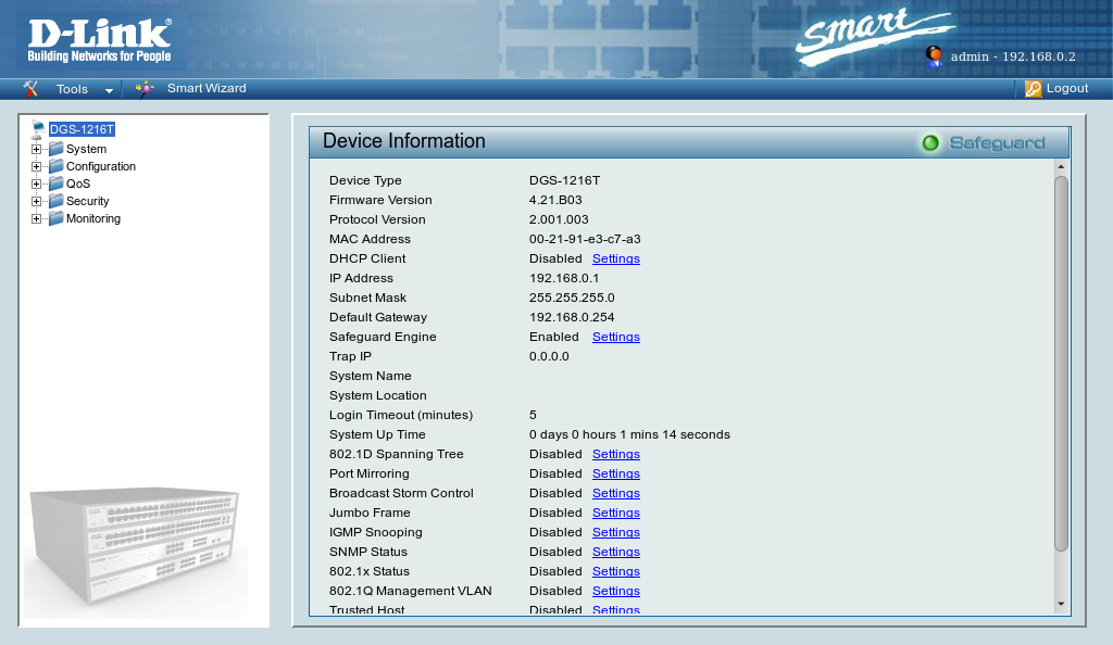
Success! Finally we unplug all the debugging cables and see if the switch is now happy – it is:
 In desperation I looked at the Xerox wax printers. If you’re not familiar with the technology, they work by melting blocks of wax and then squirting the molten wax onto the paper using a piezoelectric head (rather than boiling the ink’s solvent as most inkjets do). This has the advantage, as the ink is already a liquid and doesn’t need a solvent, that the nozzles won’t clog as the solvent evaporates. You can pick up a used ColorQube (presumably misspelled for legal reasons) 8570 fairly cheaply, and they weigh in at a reassuring 27.4kg. Better still a service and maintenance manual is available.
 There’s a sensor in the printer that determines if there is or is not a notch at the locations “B”, “C” and “D”. The chap at PyroBrit spent some time working out what the various combinations mean:


 The simplest modification is to remove the output for the D position and connect all the sensors together, then ink at any position will register as positions B and C (European). The modification looks like this:


 l
l